According to the rules of the graphics card market, this device may not have been available for sale for at least another six months. But AMD decided to use against NVIDIA accelerators main weapon, which currently have a red team - the advanced process technology 7 nm. We'll see, is that enough, to the updated chip Vega toppled from its pedestal GeForce RTX 2080
Introduction
In recent years, we have become accustomed, that AMD has consistently taken the position in the competition with NVIDIA catching. Last time, When playing the video card under the brands GeForce and Radeon had equal opportunities in the upper price segment, It was in the days of GeForce GTX confrontation 980 Ti и Radeon R9 Fury X. The weakness of AMD graphics division and architecture Graphics Core Next, which has existed for almost a decade, It became especially noticeable after, like NVIDIA released GeForce RTX Series device. The brainchild of Jen-Hsun Huang is not only reigns supreme on the market of high-performance GPU, but it sets the course of development of the industry at the expense of ray tracing technology in real-time and machine learning.
By AMD honor, in the budget and mid-class gaming graphics its products are still in demand, and models of family Radeon RX Vega proved themselves as accelerators general purpose calculations. And now the "red" one more reason for optimism: Senior GPU Vega family migrated to progressive standard 7 nm FinFET. Updated Chip Vega 20, which was presented to the public in the fall as part of accelerators computing Radeon Instinct, He became the first discrete GPU, produced by this technology, while NVIDIA only recently debugged production at a rate of 12 nm.
Considering, How far ahead of rival AMD was on the pace of development of new technological processes, Only the most loyal supporters of the company can expect a gaming graphics card, based on silicon Vega 20. But sometimes even the most daring dreams come true, because AMD has decided to do just that. What is it - a show of force or act of desperation? try to find out.
GPU
The main innovations, that characterize the second generation silicon Vega, directly caused by the transition from the node 14 nm FinFET in 7 nm. Vega chip production 20 engaged TSMC Taiwan - seems, that in this, AMD had no choice, ведь GlobalFoundries, which now produces most of the graphics chip architecture Graphics Core Next, He turned the work on its own line 7 nm, and Samsung has launched its later, than Taiwanese.
"Upgrade" GPUs through a new process technology or just a circuit design improvements for AMD already has become a tradition. Take Polaris family of chips: the eldest of these GPU - Polaris 10 - Not so long ago I survived his third birth, It has technology 12 nm. However, the chip standards 14 and 7 nm differ from each other much more, than 14 and 12 nm. At TSMC has never been a production line 14 nm, but in order, to assess the scale of the changes, which has undergone a graphics processor Vega, you can take as a starting point the characteristics of process technology 16 nm at TSMC factories. By comparison, standard 7 nm 3,2 doubles the density of chips, and power consumption is reduced by 61 %.
These numbers are unattainable in practice, because not all chips are scaled so well, all the more so complex, like modern processors, Whether it's CPU or GPU. However, AMD was able to reduce the area of its flagship chip is exactly half - from 495 to 331 mm2, despite, that it was on the 0,7 billion transistors More. How did that affect the clock frequency and the specific power of a chip, we discuss the example of most video card Radeon VII, but miniaturization GPU gave Vega 20 Another important advantage.
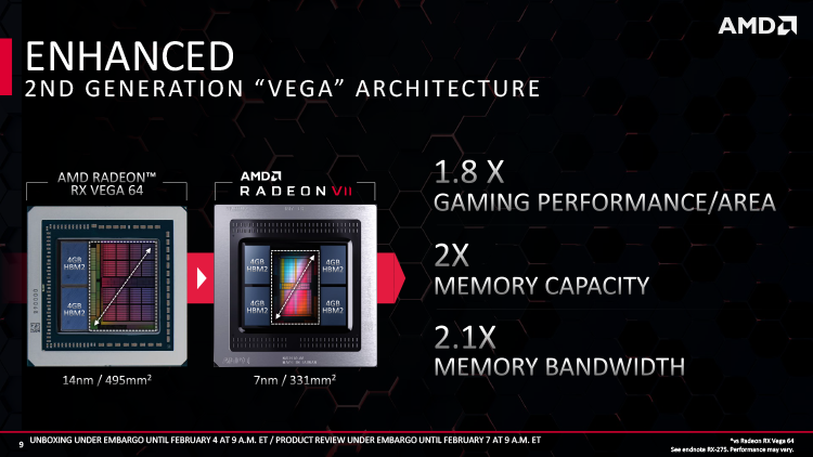
The accelerators of the top echelon of AMD has long abandoned in favor of GDDR memory chips HBM, are placed together c GPU on the silicon substrate (interposer). The latter is actually a reduced chip, in which there is only a line conductors and no transistors. Consequently, substrate produced on a standard photolithographic conveyor, and its size is limited photomasks. After recording Vega 10 good visibility, that the GPU giant AMD is simply not allowed to place on the substrate more than two stacks HBM2. That is why Vega 10 half the bit width of the memory bus of the chip is relatively Fiji (the first GPU, where AMD used the memory HBM), even increase the frequency of second-generation HBM compensate involuntary step back.
On the other hand, on the substrate around Vega 20 It has plenty of room for the four assemblies HBM2. AMD took the opportunity, at the same time to double capacity (which now stands at an incredible performance in 1 Tb / s) and RAM: accelerators computing Radeon Instinct on chips Vega 20 We got up to 32 GB RAM, а Radeon VII - 16 GB.
The focus of the additional memory controllers as 0,7 billion transistors, who appeared in the new version of the processor, but GPU architecture has undergone other changes. AMD worked on the assembly line efficiency - as in 3D-rendering, and calculations of general purpose. In particular, productivity was increased ROP blocks, so that they can take full advantage of the expanded memory bus, and from the shader ALU - execution speed FMA (Fused Multiply-Add), perhaps the most important operation for a variety of computing tasks. The rest of the Vega 20 still belongs to the fifth generation GCN and contains no changes to the ISA level (Instruction Set Architecture). The last feature of the chip, What is worth mentioning, It is the fulfillment of a double-precision calculations (FP64) at speed 1/2 of peak performance in FP32. In theory, this ability to have any accelerators GCN architecture, but at the design stage AMD decides crystal, how much FP64 speed will be limited in accordance with market positioning device. But since the main purpose of Vega 20 GPGPU applications are (General Purpose GPU), This feature has not been trimmed in the silicon level,.
Specifications, price
Although the graphics processor Vega 20 It corresponds to a set of principal computational units from older "Vega" first generation, Radeon VII did not get a fully functional version of the GPU. Chip Vega 20 in a configuration with 64 active CU (Vega 20 XT) while you can only find on the board Radeon Instinct MI60, but as part of Radeon VII used the same version of the Chip, in Instinct MI50 - Vega 20 XL. It remains 60 CU-bodied, which means 3840 shader ALU (stream processors, AMD's terminology) and 240 texturing units. If we make a comparison with the previous generation model range, the Radeon VII stands exactly halfway between the Radeon RX Vega 56 и Vega 64, so AMD has still remained the possibility to release a more powerful video card, if the company deems it appropriate.
In, graphics processor Vega 20 It appeared on the consumer market in a "stripped-down" version, not surprising. The yield of chips with as many transistors in the norm 7 nm has certainly leaves much to be desired, and full-bodied crystals AMD cares for its server products. On the other hand, there is no reason for disappointment, because the gamer version Vega 20 retained 94 % its full computing power. Judging by, both games are related Vega 56 и Vega 64, but they differ in terms of hardware is much stronger, loss of four Compute Unit'ov Radeon VII definitely survive.
| Manufacturer | AMD | |||
|---|---|---|---|---|
| Model | Radeon RX Vega 56 | Radeon RX Vega 64 | Radeon RX Vega 64 Liquid Cooled | Radeon VII |
| graphics processor | ||||
| Title | Vega 10 XL | Vega 10 XT | Vega 10 XTX | Vega 20 XL |
| microarchitecture | GCN 1.4 | GCN 1.4 | GCN 1.4 | GCN 1.4 |
| Tehprocess, nm | 14 nm FinFET | 14 nm FinFET | 14 nm FinFET | 7 nm FinFET |
| the number of transistors, million | 12 500 | 12 500 | 12 500 | 13 200 |
| Clock frequency, MHz: Base Clock / Boost Clock | 1156/1471 | 1247/1546 | 1406/1677 | 1400/1750 |
| Number of Shader ALU | 3584 | 4096 | 4096 | 3840 |
| Number of texturing units | 224 | 256 | 256 | 240 |
| The number of ROP | 64 | 64 | 64 | 64 |
| RAM | ||||
| bus width, bit | 2048 | 2048 | 2048 | 4096 |
| chipset type | HBM2 | HBM2 | HBM2 | HBM2 |
| Clock frequency, MHz (bandwidth per pin, Mbit / s) | 800 (1600) | 945 (1890) | 945 (1890) | 1000 (2000) |
| volume, MB | 8096 | 8096 | 8096 | 16192 |
| I / O bus | PCI Express 3.0 x16 | PCI Express 3.0 x16 | PCI Express 3.0 x16 | PCI Express 3.0 x16 |
| Performance | ||||
| Peak performance FP32, GFLOPS (calculating from said maximum frequency) | 10544 | 12665 | 13738 | 13440 |
| Performance FP32 / FP64 | 1/16 | 1/16 | 1/16 | 1/4 |
| Bandwidth RAM, GB / s | 410 | 484 | 484 | 1024 |
| image output | ||||
| image output interfaces | HDMI 2.0, DisplayPort 1.4 | HDMI 2.0, DisplayPort 1.4 | HDMI 2.0, DisplayPort 1.4 | HDMI 2.0, DisplayPort 1.4 |
| TDP, W | 210 | 295 | 345 | 300 |
| Retail price (USA, tax free), $ | from 329 (newegg.com) | from 399 (newegg.com) | from 599 (amazon.com) | 699 (recommended at the time of withdrawal) |
The transition to "thin" the norm 7 nm allowed to radically increase the clock frequency: operating range Vega 20 board Radeon VII is 1400-1800 MHz. curious, that it is the last number used in official materials, when it comes to the upper frequency, available video card, while the first-generation accelerators Vega often characterized by the term Boost Clock (maximum frequency at typical processing load), as well as the new "Vega" on potyazhelela 0,7 billion transistors. Seem to be, AMD than ever convinced of the merits of the new process technology.
However, apart from the absolute figures and compared with the Radeon VII Vega 64 in percentage terms,, AMD is able to accelerate GPU only 10 % at the maximum frequency, and intergenerational difference in bandwidth shader operations standard accuracy (FP32) and texturing speed is 12 and 7 % respectively - not so much even after adjusting for the four missing Compute Unit'a. But of course, in recent years it has become ever more apparent, that the title "nanometrazh" (transistor gate length) - it is not a complete description of the photolithographic process. So we can not talk confidently about, how much silicon, released at a rate of 7 nm at TSMC factories, It must be different in theory from the 14-nanometer chips Vega 10 production GlobalFoundries.
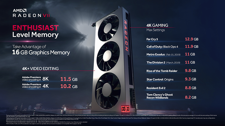
Howbeit, AMD says, that the performance of Radeon VII on 25 % above, than the Vega 64 with equal power consumption, and the average increase in FPS games is from 20 to 42 %. So it is true or not, we learn from the test, but it is known, where are these numbers: with four channels HBM2 memory chip Vega 20 It has a memory bandwidth of more than two times higher than the Vega 10. A gap between the largest values and novelty Radeon RX Vega 64 It reaches in the case, when an application can master more than 8 GB VRAM. However, for Radeon VII 16 GB of memory - it's mostly reserve for the future, because until only a few games, and only in the 4K mode with aggressive graphics quality settings are beyond 8 GB. Another thing - working applications for 3D-rendering, video editing, and similar demanding tasks, in which Vega has some great architecture shown, but it was often limited to the local memory.
As soon as we were talking about a general-purpose computing, worth noting, Radeon VII that has a unique opportunity for its price to perform the operation of double precision (FP64) at speed 1/4 the bandwidth in FP32. As I mentioned above, in the chip Vega 20 This characteristic is 1/2 by FP32. The consumer version of AMD silicon decided to artificially limit, but even in such a Radeon VII is unparalleled in terms of price / performance in double-precision calculations. At the same time in order, to leave between the Radeon VII and accelerators family Radeon Instinct appropriate distance, novelty relieved of a number of other regalia server product: in particular, there is no Infinify Fabric bus connectors to connect multiple GPU cluster, and support for PCI Express of the fourth generation - the lack of a lot of the latest discouraging in light of the, that the future platform Zen 2 It will use it to the fullest.
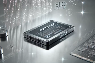
Radeon VII went on sale at a suggested cost $699. Price clearly points to the graphics card rival firm, with which the new product will have to fight in benchmarks - GeForce RTX 2080. AMD confirms, that the game speed, these devices are equivalent. Like it or not, we learn today. But if there is an opportunity for AMD to meet the demand for Radeon VII by hungry fans, It is still an open question. Price almost $700 - a record for a single-processor accelerators Radeon. However, according to unofficial, but completely convincing calculations of production of one copy Radeon VII (taking into account the yield of chips at a rate of 7 nm, and the current prices for memory HBM2) costing the company in $650, and at first the video card is in severe deficiency.
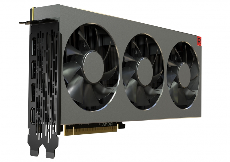
Design
The reference accelerators "red" chips, designed for mass production, never differed refined design. AMD engineers (rather, SAPPHIRE, it is this company has always released for the AMD reference designs) We can not be accused of neglecting quality, but, usually, about the aesthetics of the product they are thinking in the least - even if it comes to such expensive and in some ways things status, as a high-performance graphics card. The only exceptions were some modifications Radeon RX Vega (limited series Frontier Edition, Limited Edition и Vega 64 Liquid Cooled), the high price justifies Manufacturer expenses for design and expensive materials. However, Radeon VII is also not designed for the mass market, for AMD is primarily a signal of willingness to fight for the market for higher-tier video cards. This means, the device should make a good impression when meeting.
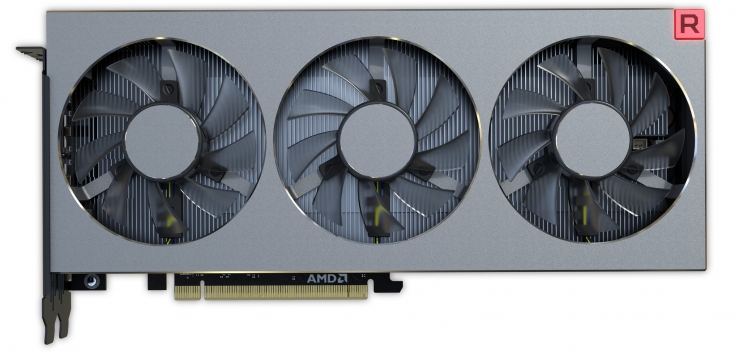
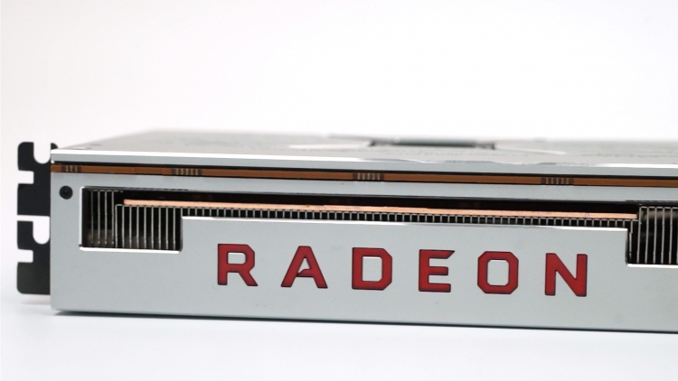
In the guise of Radeon VII heard the same "design language", but that says "premium" version of Radeon RX Vega. video sheath entirely made of anodized aluminum, but because there was only plastic elements Radeon logo and cube with the letter R in the corner of the building - and then, and the other is red, when the device is powered. Notably, that even on the cooling fans have aluminum cover.
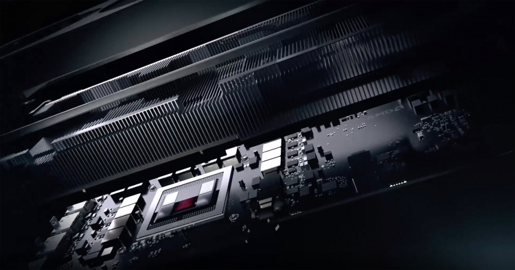
But, of course, the main difference from the previous Radeon VII reference cards in large chip architecture GCN, This cooling system is open. At SAPPHIRE gets a good cooler with radial fan - even Vega 64 with a standard power in the region 295 W is serviced such CO. Weak point "impeller" - a noise level, and as soon as Radeon VII crossed the mark of 300 W, AMD had to create a reference for the design of more efficient versions.
The length of the circuit board and the housing Radeon VII - the novelty of these parameters is not different from Vega 64 - allowed to place on the radiator three impeller diameter 75 mm. In comparison with the majority of fans, who used AMD and NVIDIA partners in the devices of the original design, SAPPHIRE chose unusually powerful model, which may develop higher speed 3000 rev / min - looking ahead, recognize, that the new product is very suitable, but about temperature control chip Vega 20 we talk later.
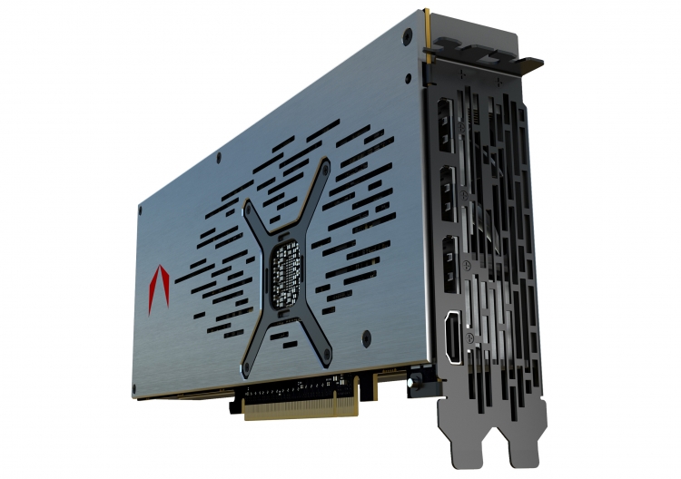
Compared with the reference version of Vega 64 AMD's new flagship has grown in width: Now housing advocates panel border with video outputs. This is primarily due to the increased board space, and at the same time under the front panel of the casing there are more places for the GPU heatsink. Coolant Radeon VII arranged solidly, but disappointingly just: GPU and memory chips are covered HBM2 evaporation chamber, and distribute heat on the radiator fin to help five flattened heatpipe width 10 mm. AMD has done without such frills, as the evaporation chamber to the entire board space, and voltage regulator components are cooled by a flat metal frame. The last part is separated from the main radiator: between it and the bottom surface of heat pipes have contact, but it is hardly conducive to heat transfer, tk. in between there is no thermal spacers.
In general we can say, cooler new design is worthy of such a powerful cooling and hot GPU, like Vega 20, but it is unlikely to manifest in the extraordinary effectiveness tests. Anyway, for 300 Watts in Radeon VII fairly small heatsink, and the direction of the radiator fins and closed form of the housing allow air to produce only perpendicular to the motherboard.
However, these shortcomings to some extent compensates for unusual termointerfes between the heatsink and the GPU chip. Instead thermopaste base vaporization chamber is covered with a special composition dense. With AMD known words, it's thermal pad Hitachi TC-HM03-based graphite fibers. But with conventional thermal spacers, which Radeon VII pasted on FETs VRM, it has little to do. Passport thermal conductivity Hitachi TC-HM03 (25-45 W / mK) significantly higher, than that of high-quality mineral thermal paste (12,5 W / mK). The only disadvantage of this solution is, that the gasket can not be reused after removal of the radiator - the material necessary breaks and not the fact, that it can be replaced by an ordinary thermal grease. The fact, that the gap between the sole and the evaporator chamber surface GPU designed for lining thickness - after, as a user removes lumps with chip Hitachi TC-HM03, will have to apply thermal grease excessively thick layer, and there is no guarantee the uniformity of the heat sink clamp. In theory, can increase the pressure due to the screws on the back side of PCB, but they, it seems, the already twisted to the ground.
Among the first owners of Radeon VII sure there are brave, who dismantled the cooling system, and then we will know, Whether the new product allows secure change thermal interface. But we decided to keep a potentially expensive and scarce unit, leaving the heatsink in place.
Printed circuit board
Since we did not disassemble the test sample Radeon VII because of fears interfere with the operation of the cooling system or split the GPU as a result of replacement of the thermal interface, and AMD did not provide photos of the internal graphics device, in this regard had to resort to third-party sources. However, PCB samples of various Radeon VII unlikely to differ within the same party, and only the front surface of the photo bears almost all the information of interest to us.
Thanks to, that stacks HBM2 RAM arranged on a common silicon substrate with the GPU (Unlike the first samples Radeon RX Vega 64, the gaps between the chips already filled epoxy compound), significant portion of the PCB in Radeon VII vacant, but immediately obvious, for what purpose the PCB made wider in comparison with the reference model Radeon RX Vega. Additional area needed for, to accommodate the components of the power system enhanced. There is a seating area for chokes, capacitors and MOSFET'ov sixteen separate phases. AMD has not only refused to dual driver FETs, but applies costly field-effect transistors with integrated driver (DrMOS). Besides, PCB Radeon VII unusually thick - perhaps thicker, than any other graphics card, with which we have dealt. And since the tracks on the board to communicate with the RAM chip Vega 20 Not needed, the reason probably in voltage regulator.
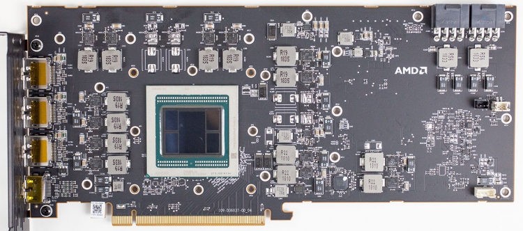
However, VRM sixteen phases Radeon VII uses only twelve - one less, than reference boards of the first generation Vega. Judging from the layout, ten phases designed for the GPU and two - for HBM2 memory chips. Power is supplied via two Eight-connector, and hence power, that Radeon VII can learn under the current, on which these vehicles are designed with PCI Express slot, is 375 W. Judging by, that the video card BIOS allows you to increase the power of full-time 300 W 20 % (up to 360 W), AMD complies with the specification data.
Completing physical examination of trends, we note that the on-board Radeon VII no two components, without which in recent years does not do any one high-card AMD - power indicator in the form of LED bar next to the power connectors and, more importantly, backup BIOS chip.